By Miranda Li
YMTC has recently delivered samples of its self-developed 192-layer 3D NAND flash memory to some customers and is expected to officially launch the products later this year, according to industry sources.

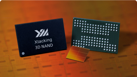
YMTC developed flash memory based on its advanced Xtacking architecture. The most prominent feature is that the interface transfer rate is extremely high, reaching 3GT/s, far better than the general 1.6-2.0GT/s, according to news from Kwai Technology.
YMTC's patented Xtacking architecture enables the processing of periphery circuits and the memory cell array on two separate wafers using the logic technology node, supporting the desired I/O speed and functions. With Xtacking, the periphery circuits are above the array chip, enabling a much higher NAND bit density than conventional 3D NAND.
Established in Wuhan, the capital of central China's Hubei Province, in July 2016, YMTC (长江存储) is China's leading IDM of 3D NAND flash memory with comprehensive memory solutions.
YMTC has entered Apple's supply chain and has supplied memories to the company's newly released iPhone model, as reported in the Chinese press in March this year.
The U.S.-based research firm Tech Insights said that the storage density of YMTC's 128-layer TLC 3D flash memory had reached the industry-highest 8.48 Gb/mm in the last October report.
Micron Technology, a U.S.-headquartered world leader in memory solutions, was reported to have launched the world's most advanced and first 232-layer 3D NAND flash memory, which will start ramp production in late 2022.
Market watchers believe that Samsung Electronics will join the race to provide 3D NAND flash memory of more than 200-layer later in 2022.


