


By Greg Gao
Chiplet, the new emerging approach to make semiconductor chips more efficiently, has received more attention in China’s semiconductor industry. Panelists attending a recent online forum on the subject concluded that Chiplet represents great potential for China.
JW Insights and Shanghai Zhangjiang Hi-Tech Park jointly organized the forum in late May attended by industry heavyweight professionals from companies engaged in IP development, IC design, investment, packaging and test services, and EDA tools.
Lao Yao, JW Insights’ chairman and founder, pointed out that China’s companies have actively participating in Universal Chiplet Interconnect Express (UCIe) since its March 2 establishment by the world’s biggest chipmakers including AMD, Arm, Qualcomm, Meta, Google Cloud, and Microsoft. Many Chinese professionals believe that it will have a profound impact on the country’s semiconductor industry development.
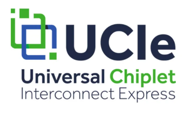
The UCIe goal is is to create a standard for connecting Chiplet together, making it easier to mix and match different Chiplet components when building SoCs.
Yu Daquan, chairman of Sky Semiconductor(厦门云天半导体), pointed out that with the rise of Chiplet in the future, chip design is expected to be further simplified into a combination of IP core stacking, and the semiconductor manufacturing chain may be reconstructed. For system providers, Chiplet can make it switch from purchasing chips to developing chip products by itself.
Yao Yao, deputy general manager of Synopsys China, also believes that Chiplet will bring revolutionary changes to the entire semiconductor industry chain. Packaging and testing service vendors and substrate manufacturers may benefit the most from Chiplet in the near term. In the medium term, Chiplet will promote the SoC concept from System-on-Chip to System-of-Chips. In the long run, the technology will provide chip manufacturers with the benefits of flexibly expanding SKUs and greatly improving yields, and attracting more companies to explore business models for single-function die.
Chiplet technology has many superior characteristics such as a fast iteration cycle, low cost, and high yield. The new technology could allow companies to build processors out of Lego-like method, which is especially suitable for Chinese system design enterprises, Dai Wenliang, co-founder of Chinese EDA software provider Xpeedic Technology(芯和半导体), concluded. The company recently joined the UCIe as the first Chinese EDA company to join the standard.
Fu Yong, the founder of ShunyaoCAD, a Shanghai-based EDA startup, believes that Chiplet will bring another major change to chip design and verification methodology after SoC. He noted that Chiplet, along with innovations in the design process such as Chisel derived from RISC-V, has further increased the scale of designs that can be handled by a single engineer.
For Chinese chip manufacturers, the ability to change technical specifications and business models are the keys to grasping new opportunities. Chiplet can realize a more specific design at a lower cost, which may become another major methodological change in semiconductors after SoC. The technology innovation brought by Chiplet is expected to enable China’s domestic design companies to give full play to their system product R&D know-how, Fu Yong noted.
Meanwhile, Chinese semiconductor players also face daunting challenges. Yu Daquan emphasized that Chiplet is not equivalent to advanced packaging, and certain products do have extremely high requirements on packaging technology. At present, Chinese mainland manufacturers have a gap of several generations in advanced packaging technology compared with industry-leading companies like TSMC. The gap should be narrowed through closer collaborative innovation of industry-university-research institutes.


RELATED
-
China releases its first CPO technology standard, a derivative of chiplet standard
08-08 11:33 -
China’s leading OSAT company JCET Group achieves high-volume packaging of 4-nanometer chips by leveraging Chiplet technology
08-04 15:38 -
SCMP: China’s natural science fund supports new ‘chiplet’ tech research to advance semiconductor self-sufficiency amid threat of new US sanctions
08-04 14:11
READ MOST

No Data Yet~