


By Gabby Chen
SMIC (中芯国际), China’s leading IC manufacturer, successfully completed the main structure of its 12-inch wafer fab in Lingang Special Area of Pudong in Shanghai on December 29. It is SMIC’s first such large-scale logic chip foundry built in Twin Fab method, JW Insights reported.
SMIC’s new fab is designed for 12-inch wafer fabrication with a monthly capacity of 100,000, as part of its plans for ambitious expansion.
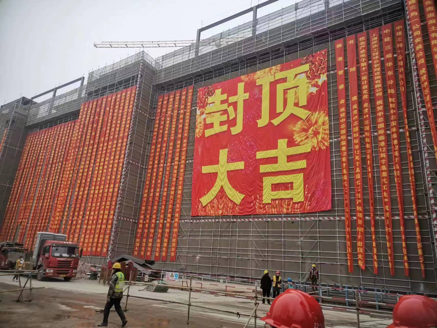
The project was implemented by a joint venture company between SMIC and the management committee of Lingang Special Area of China (Shanghai) Pilot Free Trade Zone, with an investment up to $8.87 billion. They reached the cooperation agreement on September 3 last year, according to SMIC’s announcement.
The joint venture company has a registered capital of $5.5 billion, of which SMIC will contribute at least 51%, and the Shanghai municipal government proposes to invest no more than 25%, the announcement noted.


RELATED
-
Chinese top-tier chipmaker HuaHong Semiconductor's net profit plummets 86 percent in the third quarter
11-17 19:11 -
Chinese MEMS provider Fatri UTC will set up its sensor chip production plant in Shanghai
11-16 18:30 -
China's packaging and testing services provider Forehope Electronic will build a new plant with RMB2.157 billion investment
11-15 17:17
READ MOST

No Data Yet~