


By Kate Yuan
Hefei, the capital city of eastern China’s Anhui Province officially started construction of the IC Testing Industry Base on March 21 for 8-inch and 12-inch wafers, according to the local ahwang.cn report.
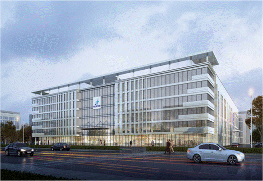
Source: ahwang.cn
Hefei Huayu Semiconductor (华宇半导体) manages the testing base – a key project in the Hefei High-tech Zone. The construction area covers about 50,000 square meters, including workshops for production, assembly and supporting facilities.
The designed capacity for the project is 90,000 pieces per month and 100 million pieces of high-end IC chips per month. The planned completion schedule is May 2023.
Hefei High-tech Zone has seen remarkable achievement in the IC industry in recent years, having attracted many companies since its completion in December 2020 with the annual output value at RMB500 million ($78.5 million).
Ahwang.cn also reported an IC Company Headquarters Base is under construction with RMB1.8 billion ($0.3 billion) investment and a total construction area of 334,000 square meters. It is intended for companies engaged in IC design, packaging and testing, smartphones, and IoT, with a goal to be among the advanced IC industry bases in the country.


RELATED
-
Volkswagen's EV plant in southern China's Hefei is to start production with a maximum annual capacity of 350,000 vehicles
09-22 13:30 -
German firms double down in NEV cluster of eastern China’s Hefei City
08-30 17:08 -
JW Insights becomes one of the first global partners of USTC Silicon Valley Project in eastern China’s Hefei
08-09 16:39
READ MOST

No Data Yet~