


JW Insights Tech Forum
Editor’s Note: “Tech Forum” is a new section of our English website. It will feature in-depth technical articles instead of news reporting by our analysts and guest experts in China’s mainland and around the world including Taiwan region. As our first article, “Why Advanced Packaging Materials Matter?” gives the insights in two parts on this new frontier of semiconductor technology developments.
JW Insights Tech Forum: Why Advanced Packaging Materials Matter?(Part A)
JW Insights Consulting
I. Evolution of Advanced Packaging
a. Packaging Fundamentals-Technology Hierarchy
Microelectronic packaging is an important segment in the semiconductor manufacturing value chain. It is an interdisciplinary engineering field that requires electrical, mechanical, chemical and material knowledge to deliver interconnection solutions for functional electronic products.
Electronic packaging provides electrical interconnects, mechanical support, and thermal management solutions to ensure the performance targets of an electronic system is attained. There are three levels to a generic packaging hierarchy (Table 1). A wide variety of materials and processes are used to make products ranging from IC packages and modules to complete computer systems.
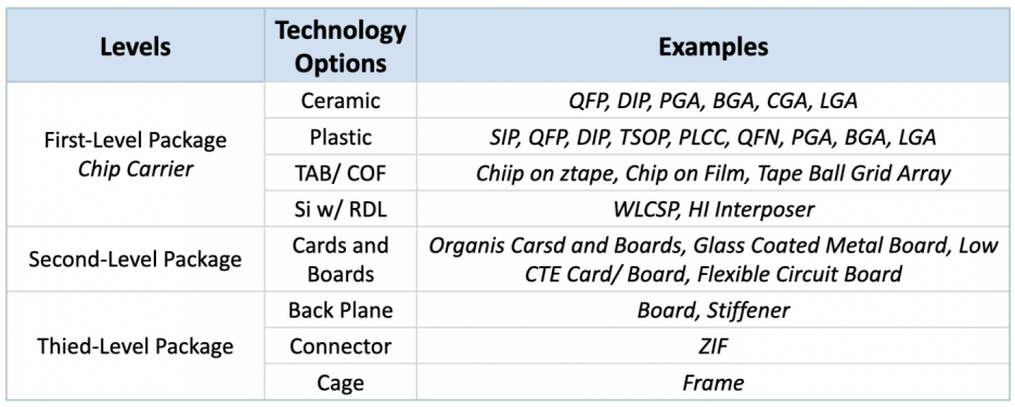
Table 1. Packaging Levels
As shown in Table 1, many first level package types in different form factors are available for semiconductor die assembly. There are five major types of carriers currently in use: metal leadframe, ceramic carrier, organic substrate, silicon interposer w/RDL (Redistribution Layer) and flex tape. Metal casings, made of Kovar® for example, are commonly used for making hermetically sealed packaging for specialty applications.
Three techniques are commonly used to achieve connections between the IC chip and carrier are wire bond, solder and flip chipconnections. Currently, wire-bonded products claim about 70% of market share based on unit count.
The majority of IC devices now are assembled as plastic packages, in which either a leadframe, or organic substrate is used as carrier. After die attachment and electrical connection, a molding operation using epoxy thermoset resin (EMC) completes the encapsulation process. As multicavity mold chase can be designed to produce many packages in one step, which offers a distinct cost advantage for volume production.
The packages are designed to use leads, pins and pads for the next, second, level of connection to printed circuit cards, boards and flex tapes. Through holes and surface mounts are completed by soldering and the use of sockets provides ease of replacement.
The key material properties used for packaging applications are summarized in Tables 2 and 3. These are the building blocks for use in various packaging types. There are many selections; however, it is especially important to recognize that majority of organic dielectrics are polymeric resins made from composite mixtures. As a package’s performance and reliability are strongly affected by material properties, a detailed knowledge needs to be accumulated to select and process these materials properly
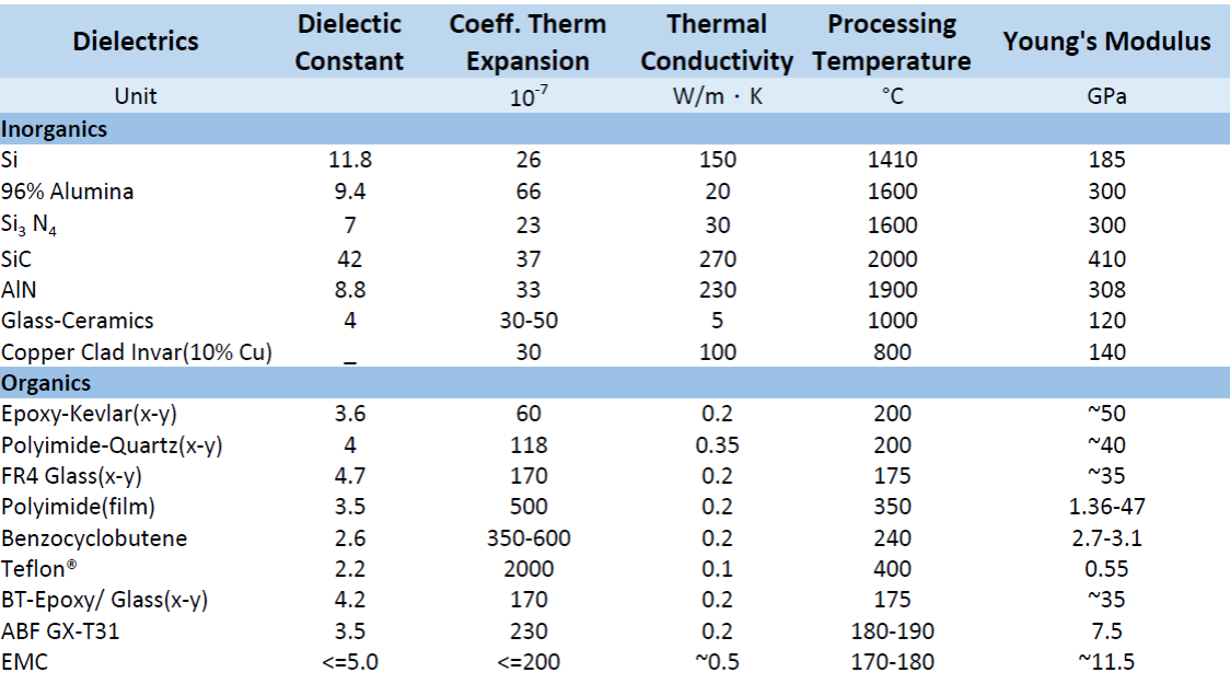
Table 2 Packaging Material Properties-Dielectrics
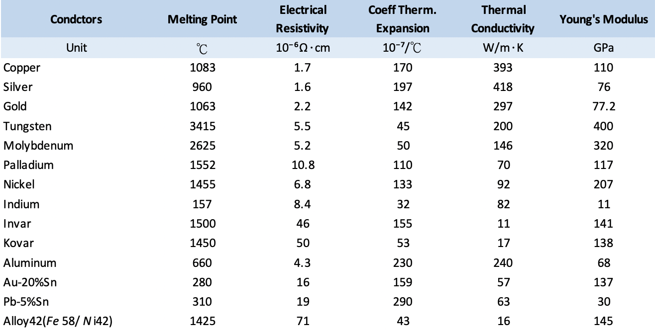
Table 3 Packaging Material Properties-Conductors
Several key milestones worth mentioning related to packaging technology development are as follows:
b. Key Technology Milestones:
i. Flip Chip Process
C4 (Controlled Collapse Chip Connection) Bump.
The flip chip method, also known as C4 or Controlled Collapse Chip Connection, was first used by IBM in the 1960s. A silicon transistor and diode planar chips are mounted face down on a pinned ceramic substrate using Cu balls and solder to form a SLT (solid Logic Technology) module. Later development led to a set of reliable UBM (Under Bump Metallization) and Tin (Sn)/lead (Pb) solder ball structures suitable for area array high pin count connections. Solder bumps are formed by depositing solder metals on chips using an evaporation process followed by reflow. Both logic and memory C4 chip modules were produced in volume and used in IBM’s mainframe computers.
The flip chip method offered several advantages over the then perimeter wire bonding method:
a. Reduced form factor: smaller footprint and lower profile
b. Improved electrical performance
c. Ease of thermal management via exposed chip backside
d. High I/Os density allowed by area array interconnections
e. Capability for multiple reworks
f. High productivity: multiple connections completed by one self-aligned reflow process
g. Enhanced reliability
As the first generation C4 assembly needed to be processed at temperatures higher than 300°C, it limited the selection of carrier materials to ceramics. In general, a ceramic package having a die size less than 10x10mm2 and compliant solder connections is suitable for high reliability applications without the use of an underfill resin (C4 encapsulant).
A key enabling technology, the underfill encapsulation of flip chips was developed in the 1980s to enhance the reliability of flip chip assembly. The availability of underfill resin and use of low temperature solder bumps in the 1990s brought low cost laminate based flip chip PBGA (Plastic Ball Grid Array) packages into high volume production replacing many ceramic assemblies. New development in flip chip technology continues and it has become an essential part of modern day high density packages.
Copper (Cu) Pillar Bump
The Cu pillar bump is a variant of C4 technology. With improved thermal and electrical conductivity over C4, it is an important interconnection method used in advanced packages. Having a smaller solder cap on top of a Cu standoff, the Cu pillar bump also offers an advantage of avoiding possible solder shorting between the adjacent fine pitch pads during mass reflow. However, a smaller solder volume also limits the bump’s self-alignment capability derived from surface tension. To facilitate accurate alignment, a thermo-compression bonding method is chosen to assemble Cu pillar chips with a bump pitch less than 30 microns. The Cu pillar bump interconnection is now being used in chip-to-substrate, chip-to-chip, and chip-to-leadframe packages.
Gold (Au) Bump
Gold-plated bumps can be categorized as a “pillar bump” as well. They do not collapse and it needs a matching metallurgy, gold and tin, for chip joining. It is mainly utilized for Display Driver IC (DDIC) assembly where high pin count and fine pitch (< 25micron) connections are required. (Figure 1) Typical chip attachment involves thermo-compression bonding onto display glass panel (COG, Chip on Glass) or polyimide tape carrier (COF, Chip on Film). These types of products have found applications for all kinds of flat panel displays for TVs, computer monitors, smart phones, auto displays, etc. Current global shipment of DDIC units is estimated at about seven to eight billion units per year.
Success of a material development project in the late 2000s led to the production of copper/gold composite bumps (MCB – Metal Composite Bump) (Figure 1). The resulting bump structure consists of a Cu/Ni/Au stack. This is a worthwhile option to reduce the effects of a rising gold price on material costs. Many low price mobile products are now assembled with metal composite bumped COGs display drivers.
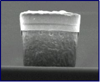
Figure 1. Au Bump and Metal Composite Bump / ChipMOS
Indium(In) Bump
Indium is a soft metal with low melting point. The indium alloy-based bump connections exhibit good fatigue life and thermal conductivity. It has found usage for many applications related to automobile and optoelectronic IC packaging.
Gold Stud Bump
Without the use of wet plating process, a gold stud bump is formed by the wire bond method, in which once a ball bond is formed on an IC bond pad, the gold wire is then severed by pulling to yield a stud standoff. A gold stud bump height is constrained by the wire diameter and wire bond pitch. Soldering is required as the next step of chip attachment. It has found only limited applications for simple flip chip packages.
Although flip chip technology was invented over 50 years ago, its applications continue to grow. The development of new materials and related bonding processes is the current focus of innovations to enhance capabilities for high-end heterogeneous integration and 3D die stacking assembly.
ii. Multichip Modules (MCM)
Multichip Modules (MCMs) were developed to provide interconnections for multiple ICs assembled in a single package. This concept has been evolved continuously to shape modern day system-level solutions.
MCMs place bare dies closely together on a substrate resulting in a higher wiring density than that of board level interconnections. MCMs thus offer major improvements in electrical performance and package size reduction.
Depending on the selection of substrate materials, three distinct types of MCM have been formally defined by IPC (Interconnecting and Packaging Electronic Circuits): MCM-C, MCM-L and MCM-D.
MCM-C: Alumina substrate has found extensive usage in MCM assembly. Early work was initiated to build hermetically sealed modules for defense and aerospace applications. To meet the demand for high-density wiring, substrates having multi-layer structures were builtby a process of green sheet sintering. Tungsten and molybdenum, which can sustain the high temperature firing process were used as conductor materials for circuitry. Interlayer connections are achieved by filled metallized vias.
The lower sintering temperature of glass ceramic materials allows the use of copper for MLC (Multilayer Layer Ceramic) wiring. Compared to alumina, glass ceramic carrier with copper circuitry exhibits improved electrical performance, lower CTE and lower dielectric constant that suitable for advanced packaging. Flip chip attached MCM modules have been employed extensively by IBM in their high-end computers. Figure 2 shows a glass ceramic MCM capable of interconnecting 100 bipolar logic chips and an example of a module interconnects logic and memory dies, four Power 5 processors and four L3 cache chips, onto a large 90x90 mm multilayer glass ceramic carrier.
Figure 2. IBM Glass Ceramic MCMs / Ceramics Art & Science (Left);WIKIPEDIA (Right)
Ceramic’s high thermal resistance allows MCM module to undergo multiple mass reflow cycles for C4 flip chip rework. This a critical requirement for MCM substrate under a situation where known-good-die’s availability is limited. However, it is affected by high fabrication cost and limited opportunities for wiring density improvement, so many of its applications are now moved to organic and silicon-based carriers.
MCM-L: Reinforced laminates derived from printed circuit board (PCB) technology are used as carrier materials for MCM-L. Multilayer wiring fabrication involves photolithography processes, lamination of circuitized core under heat and pressure followed by introduction of drilled plated through holes (PTH). Inner circuit plane connections are achieved by via, blind via and PTH. As cured organic laminate resins lack thermal resistance to endure the C4 reflow temperature of over 300°C, die and component mounting are attained by wire bonding and soldering. Finished modules protected by EMC (Epoxy Molding Compound) molding or cap are not hermetic.
Continued implementation of new materials and processes such as high glass transition temperature resin, low melting lead free solder and underfill technology enable the use of flip chip attachment onto organic substrates, such as BT (bismaleimide-triazine)-Epoxy laminate. The concept was future extended and applied to various advanced packages. For example, many SiPs (System-in-Package) now in volume production use BT-Epoxy substrate to integrate different dies and discreates in a single package. By a broad definition, they can be regarded as an extension of MCM-L.
MCM-D refers to multichip modules having conductors and dielectrics layers sequentially built on a supporting carrier by a thin film deposition process. Fine pitch wiring formed by photolithography processes delivers dense interconnections between multiple dies and circuits on the substrate. Both metal deposition and dielectric processing are often conducted at elevated temperatures, therefore materials such as silicon, ceramic and metal that exhibit good thermal stability are used as supporting structure. A common MCM-D material set includes Cu wiring, and high a temperature polyimide, PBO (polybenzoxazole) or BCB (benzocyclobutene) polymers, for example, as dielectrics. Vias, that can either be defined by photolithography, wet etching or laser ablation, are used for interlayer connections.
Among three types of MCMs, MCM-D uses thin film technology, which provides the best means of high-density wiring. Due to its high material and processing costs, MCM-D initially only had limited use for a few specialty applications. However, later development has substantially broadened the applications of thin film wiring to WLCSP and build-up RDL processes, thus silicon-based carrier technology plays many critical roles in advanced packaging.
The term Multichip Packages (MCP) is often used interchangeably with the term MCM. Most often seen in memory products, such as NAND and mobile RAM, dies are vertically stacked, and connections are achieved by wire bonding edge pads to substrate (Figure 3). In the same footprint, vertically stacked packages facilitate the delivery of greater density and functionalities. Memory devices with up to 16 stacked dies plus a controller are in production. Limited by package height restriction posed by mobile applications, MCP is also credited for the advancement of wafer thinning technology which has now become one of the critical processes of 3DIC assembly.
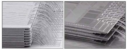
Figure 3. memory MCP staked die package / Kulicke & Soffa
MCM offers advantages in packaging efficiency, reduced physical package size and improved electrical performance. It enables the integration of multiple mixed nodes dies to deliver targeted performance. SiP assemblies for mobile products started shipment in high volume during 2000s. Various related material and process know-hows are derived from MCM technology.(校对/WM Zhang)


RELATED
-
Chinese top-tier chipmaker HuaHong Semiconductor's net profit plummets 86 percent in the third quarter
11-17 19:11 -
Chinese MEMS provider Fatri UTC will set up its sensor chip production plant in Shanghai
11-16 18:30 -
China's packaging and testing services provider Forehope Electronic will build a new plant with RMB2.157 billion investment
11-15 17:17
READ MOST

No Data Yet~