


By JW Insights
Advanced packaging technology now plays a pivotal role in extending Moore’s law of economics. It helps overcome the increasing fabrication cost and power management issues while achieving speed gains associated with the monolithic design of each new transistor node.
There are several ways to classify advanced packaging technologies. Definitions are not consistently applied across the industry. In general, they include Fan Out Wafer Level Packaging (FOWLP), 2.5D, 3D-IC, and System-in-Package (SiP). However, WLCSP, FCBGA, and FCCSP are usually included in some market surveys as well. Although currently majority (>70%) of chip packages are still assembled using wire bonding, a trend of transition to flip chip packages for high-performance products is accelerating and expected to enjoy a high market growth rate like 2.5D/3D and SiP packages in the next few years.
The use of the chiplet packaging approach allows multiple dies having discrete functions at different design nodes assembled to deliver an integrated module-level performance. As shown in Figure 1 and 2, there are various technologies one may consider to suit specific wiring feature specifications. Material selections, restricted by physical properties, processing conditions, and design rules, vary in each individual case. When package wiring density increases, there is a shift in substrate material set usage. This transition from organic substrate to silicon-based carrier is affected by several factors, such as lithography tool, reticle size, and most importantly material physical properties and processing temperature hierarchy.

Figure 1. Technology for Different Wiring Features (HIR 2021 edition)
Figure 2. An Overview of Advanced Packaging Types (Synopsis)
High-performance computing (HPC), 2.5, and 3D packaging using silicon interposers to conduct heterogeneous integration are widely adopted by the industry. For mobile computing, limited by size and package height, Package-on-Package (PoP) assembly is employed by the interconnecting application processor, memory, sensor, passive components, etc. to build a subsystem or system-level module. Various methods are used to achieve package-to-package connections, which include solder bump, TMV (Through Mold Via), Cu post (ex, TSMC’s Through-InFO-Via TiV), bond via an array (BVA), free standing Cu wire, etc.
Many materials are needed to construct the rather complex structures described above. They include process-related indirect materials such as photoresist, bonding film, solder flux, glass and metal carrier wafers for temporary bonding, etc. To complete various interconnection schemes in the package, a series of key direct materials including photosensitive RDL (Redistribution Layer) material, die-attach film, stress buffer coating, build-up film, solder paste, substrate, mSAP Cu, solder mask, etc. have been developed to meet high-density packaging requirements.
Taking solder bump connection as an example, the flip chip package has moved from high melting alpha particle emission-free tin/lead solder to lead-free SAC(Sn/Ag/Cu) and tin/silver (Sn/Ag) alloys. Copper-to-copper hybrid bonding process has now been used to enable fine pitch bonding at the silicon level such as die-to-die and wafer-to-wafer connections. Intended for low-temperature bonding processes, indium (In) and bismuth (Bi) containing alloys are being used for connecting temperature-sensitive devices.
Flip chip underfill provides protection while ensuring reliability by reducing mechanical stress on solder bump connections induced by CTE (Coefficient of Thermal Expansion) mismatch between the silicon die and carrier during thermal cycling. Formulations are usually based on epoxy or cyanate ester thermosetting resins. A filler material needs to be loaded to control the material’s CTE and modulus. Liquid underfills were first developed using liquid epoxy resin and a low-alpha fused silica mixture. After dispensing along the die edge, resin moves under the chip by capillary force and is able to form nice fillets around the die for inspection. Resin is then subsequently hardened by heat cured to complete the process. As filler geometry, amount, and coupling agent used are to influence the flow characteristic, later work involved the use of synthetic silica spheres with mixed sizes to control CTE and optimize flow properties. More development efforts resulted in no flow underfill (Non-conductive Paste, NCP), Non-conductive film (NCF), wafer level B-stageable underfill, reworkable resins, etc. to meet various advanced packaging needs. Molded Underfill (MUF) combines molding and flip chip encapsulation in one step, eliminating the need for resin dispensing and curing. It offers the advantage of production efficiency improvement; therefore, has gained acceptance in the industry. In order to enhance board-level reliability, underfill resins have also extended their usage to some CSP and BGA’s attachment processes.
To select the best fit for a given package design, many material features need to be taken into consideration. In addition to silicon, three major types of organic resin-based materials have been used as the base for circuit wiring. Figure 3 illustrated a two-die FOWLP package. The FO material set consists of silicon die, epoxy molding compound (EMC), and polyimide RDL layers with laser drilled via connections. The bottom organic carrier is made of 3 ABF (Ajinomoto Build-up Film) buildup layers on a laminate core constructed with eight layers of BT-epoxy glass prepregs having mechanically drilled PTHs (Plated Through Hole).
Table 1 shows the key characteristics of materials used to build this package. Typical values for each type of material are listed. However, physical properties do vary with a material composition that is customarily fine-tuned to meet specific processing and package performance requirements.

Figure 3. Multichip FOWLP on BT Substrate- ASE FOCoS (HIR, 2021 edition)
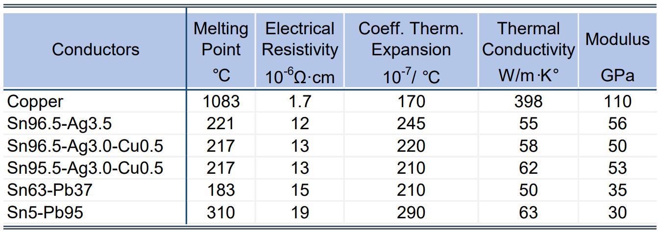
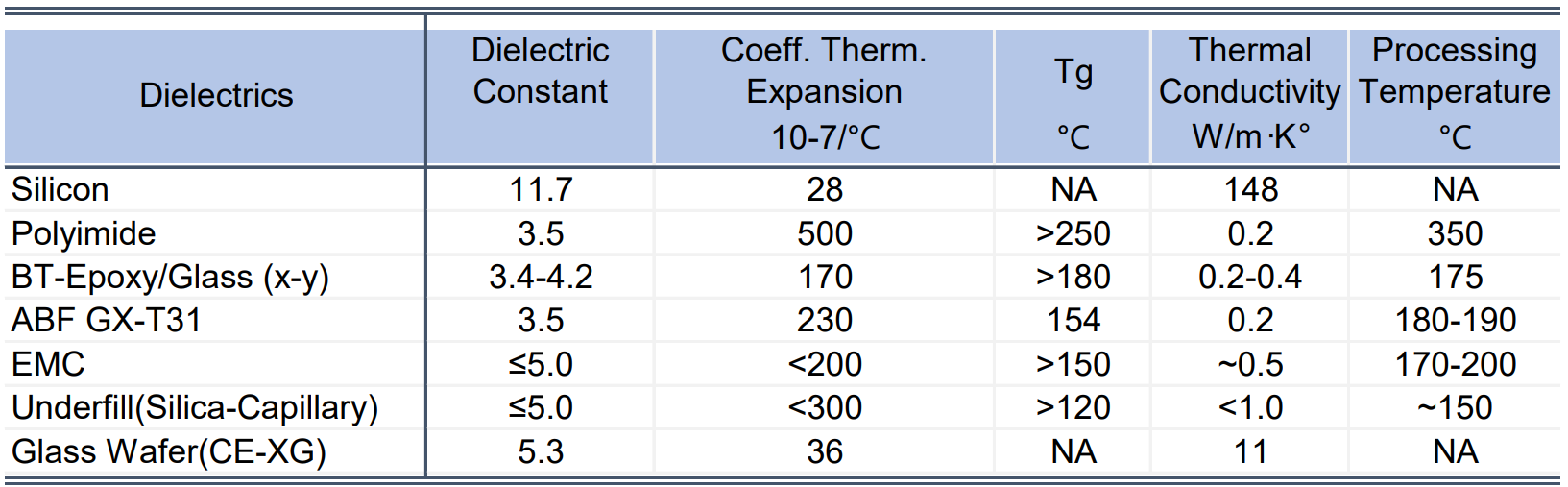
Table 1 Packaging Material Properties*Tg by DSC (NIST, INVACU, Vendor Data)
FOWLP is a fast-growing packaging type used for advanced applications. It’s derived from the WLCSP concept that was first disclosed and brought to production by Infineon in the 2000s. STATS ChipPAC (now a subsidiary of JCET) later was the first among OSATs to start high-volume manufacturing. Different from conventional WLP, the FO package for which the RDL-based connection area is larger than the chip scale, requires the use of a separate set of materials and equipment. Compared to the silicon interposer approach, FOWLP offers a less expensive choice for multi-die interconnections.
New developments have led to several process variants to yield FOWLP assemblies suitable for advanced packaging integration. It offers several advantages such as smaller size, lower cost, elimination of the bumping process, and flexibility in wiring that facilitates integration into advanced packages.
After examining the above-mentioned package in detail, one may notice that the circuit line/space feature on FOWLP, using silicon and EMC as a base, is much smaller than those shown on the organic chip carrier built upon BT-epoxy laminate. This substantial difference is also well illustrated in Figure 1 and 2.
Forming fine pitch wiring with accurate multilayer registration requires the use of dimensional stable carriers. In this regard, silicon compared to the organic substrate as shown by previous examples, would be a superior choice. This is because various complex factors inherently affect the dimensional stability of organic BT substrates. These could include resin formulation, laminate thermomechanical properties, processing conditions, and environmental effects. We are to discuss related subjects in more detail:
BT Substrate
a. Resin Formulation
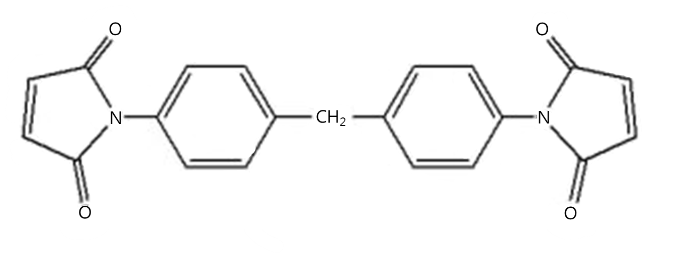
BT stands for Bismaleimide-Triazine. It’s a thermosetting formulation consisting of two components, bismaleimide and cyanate ester resin. Chemical structures are shown in Figure 4. Triazine refers to the reaction product of cyanate ester via cyclotrimerization reaction after thermal curing.
A
B
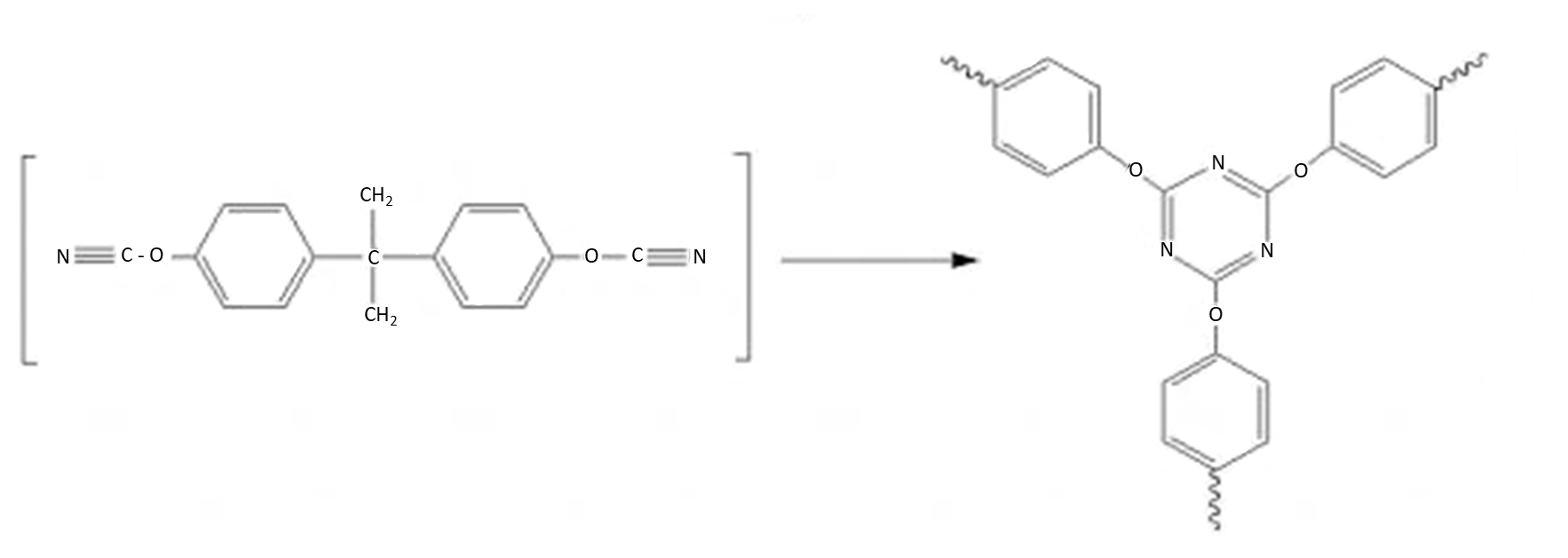
Figure 4. BT resin components-Bismaleimide(A) and Triazine formationfrom bis-Cyanate Ester(B)
i. Bismaleimide Resin
Bismaleimide is a type of polyimide having a preimidized chemical structure that doesn't produce volatiles during cure. Because it exhibits excellent thermal resistance and can be processed using the same equipment as conventional thermosets, this class of resins has been formulated with diamine curing agents and used for aerospace advanced composites and printed circuit board applications.
ii. Cyanate Ester Resin
The development of cyanate ester resin technology began in the 1960s. Monomers were first successfully synthesized from aromatic phenols. Most commonly in use is based on dicyanate derived from bisphenol A, which is also a raw material for many epoxy resins. The first dicyanate resin, Triazine A, was introduced to the circuit board industry in the mid-1970s. Cyanate ester resins can be mixed with a wide variety of thermosets such as epoxies, bismaleimides, or acrylates to form compatible blends.
This type of resin demonstrates superior electrical properties to epoxies. Cured resin’s dielectric constant and loss factor are lower than that of FR-4. Various cyanate ester-based formulations have been developed and found applications specifically for microelectronics packaging applications, which include: underfill, coating, adhesive, encapsulant, chip carrier substrate, buildup dielectric film, printed circuit boards (PCB), photoresist, etc. They have been included in formulations for a wide range of applications in the advanced composites industry as well.
iii. BT Laminates
By mixing with methylene dianiline bismaleimide, Mitsubishi Gas Chemical Company first developed a cyanate ester-based BT resin system. BT substrate is an extension of printed circuit laminate technology. Basic formulations usually include the use of more than 50% by weight of epoxies resins.
BT-epoxy blends show good solubility in organic solvents such as methyl ethyl ketone (MEK) for impregnation processing. BT substrate used for chip carrier applications is a composite laminate having glass fabric as reinforcement. Compared to conventional FR-4, BT-epoxy resins exhibit high Tg (Glass Transition Temperature) and improved thermal resistance allowing the material to withstand high-temperature assembly processing, and elevated heat operation environment. These are a few of the key characteristics that make them more suitable for chip substrate applications.
Its manufacturing process follows conventional PCB production flow. The key steps are impregnation, B-stage, prepreg lamination, and circuitization. Having a multilayer structure, the BT substrate allows the inclusion of embedded dies and passive components, such as active device, interposer die, capacitor, MEMS devices, etc.
When constructing a BT-epoxy laminate, multiple materials and process steps used inherently induced mechanical stresses affecting the material’s dimensional stability that require special attention and controls.
b. Tg and CTE
As a rule, thermosetting resin’s Tg arises along with the curing profile and stabilizes after reaching a high degree of conversion. Therefore, processing conditions affect the material’s ultimate Tg which usually is under or around the final cure temperature.
Depending on their chemical structures, pure cyanate resins readily exhibit Tgs exceeding 280°C after full cure. Consequently, this characteristic excludes the use of a conventional PCB factory’s press, with a maximum operating temperature of ~180°C by pressurized water heating, to perform lamination and complete a full cure. Therefore, a common formulation approach is by adding various levels of epoxies to lower the Tg while modifying the resin’s processibility and adjusting properties such as mechanical properties, flammability, etc. Higher Tg laminates usually require the use of elevated temperature lamination or post-cure to develop the material’s full properties.
As discussed, thermosets reach a stable Tg when complete crosslinking reaction. Cured resin goes through a phase transition from amorphous to a rubbery state when temperature elevates above its Tg. This free volume transformation results in drastic changes in resin’s modulus, elongation, and CTE that affect dimensional stability and induce stresses derived from thermal mismatch at various interfaces.
With the aid of glass fabric reinforcement, rigid laminate exhibits x-y plane CTE close to that of Cu (17 ppm/°C). This characteristic minimizes the interfacial thermal mismatch between substrate and circuitry. As the result of in-plane constrain, the substrate’s z-axis CTE normally exceeds 40 ppm/°C; thus, exerts interfacial strain in PTHs during thermal cycling. Blending low CTE fillers to the matrix resin further reduces CTEs in all directions; however, this type of formulation tends to bring more variables that need more attention during production.
Cu peel strength of BT-epoxy is adequate but slightly less than that of FR-4. However, this value is affected by several variants such as surface pretreatment, circuitization method, and types of Cu foil used.
c. Glass Fabric and Dimensional Control
The majority of BT laminates are made of E-glass fabric. Other grades of glass yarns, such as S-glass, D-glass, L-glass and fused silica, having lower CTE and dielectric constant, are produced in smaller volumes. They differ in chemical composition and physical properties. A wide selection of woven fabrics with different thicknesses, weights, and yarn constructions are available. Lightweight fabric made of fine yarn can produce prepregs with a final pressed thickness as thin as 25-35um.
Glass fabric is the key supporting element for prepreg making. The production process involves the impregnation of glass fabric with resin solution using a treater(coater). Subsequent heating removes the solvent from resin-saturated fabric to dryness and cures resin partially, resulting in a B-staged prepreg. Among several key parameters that need to be controlled are resin content, viscosity flow, and degree of curing below the resin’s gel point.
Crosslinking reactions amongst the three resin components are complicated and difficult to characterize. Various attempts were made to establish resin mixtures’ structure-property relationship. Probable mechanisms have been subjected to various spectroscopic model studies and proposed by several research groups.
One or more plies of prepregs are then sandwiched by copper foils under heat and pressure to form rigid copper clad laminate(CCL) cores for further circuitization. Resin content in prepregs made of thin lightweight fabric is generally higher than 60% by weight.
Fabrication of front-end device and RDL layers on silicon carrier use multistep processes to build up layers of circuitry sequentially. Dissimilarly, the lamination process allows to the inclusion of multiple layers of wiring using circuitized cores assembled “parallelly” together in one step. Interconnections to internal circuit planes are achieved both via and PTH.
Being a laminate composite, BT-epoxy substrate undergoes dimensional movements during manufacturing, and exposure to humidity or thermal cycles. Accurate internal layer registration is necessary to achieve reliable wiring connections., However, both impregnation and lamination steps essentially introduce many factors that influence the material’s dimensional stability and are in need of careful control. Residual stresses derived from fabric weaving, impregnation under tension, resin curing shrinkage, and prepreg lamination all contribute to certain degrees of a laminate dimensional tolerance movement and warpage.
Usually, caused by stresses induced by the glass fabric, single-ply laminate tends to warp more and be less dimensionally stable. Therefore, if thickness requirement permits, an approach is to cross-ply even layers of prepregs to balance these drawbacks. When a material set is chosen, it’s important to understand what factors influence minimal material movement and how consistently and reproducibly it moves; therefore, lithography artwork compensation may be implemented accordingly.
d. Moisture Sensitivity
Although cyanate ester resins exhibit several superior properties to epoxies, they are known to be sensitive to moisture. It is important to exclude moisture from affecting resin’s chemical reactions during prepreg manufacturing, storage, and handling. Catalyzed by organo-metallic salts, aromatic cyanates trimerize to form a stable cyanurate, s-triazine, ring structure. However, in the presence of water, aryl cyanates readily hydrolyze into carbamate moieties that release carbon dioxide gas upon heating. This side reaction induces blistering in laminates and degrades final material properties.
With proper control, full-cured BT-epoxy laminates show good moisture and delamination resistance. Existence of resin/fiberglass interface and free volume in solid resin influence moisture diffusion into the laminate. Treatment of coupling agent on fabric increases glass fiber/resin adhesion and improves moisture resistance. Moisture absorption follows the typical Fickain type II profile and desorption is complete by heat. Hygrothermal effects on the dimensional stability of laminate include x-y in-plane movement and out-of-plane warpage. As multiple components are included in laminates, warpage characteristics of a substrate are rather complicated and exert a direct impact on its capability for fine line patterning on the carrier surface. This feature needs to be properly controlled to prevent unwanted yield loss at the circuitization step.
BT-Epoxy resins are known to show good resistance to conductive anodic filament (CAF) formation. This phenomenon relates to a failure mode found in multilayer circuit laminate that metal filaments can grow from copper plated via or PTH along the glass fiber yarn to cause electrical short to adjacent cu planes. The occurrence of CAF is influenced by the presence of moisture, ionic impurities, electrical bias, a weak glass fiber/resin interfacial adhesion, and heat. CAF has been linked primarily with mechanically drilled holes in which weakened fiber/resin interface often served as an initiation point for filament growth.
The BT-epoxy laminate, frequently in combination with ABF buildup layers, has been used for a variety of applications, ranging from single chip to advanced packages such as FO substrate, PoP, SiP, embedded device/component, multi-chiplet HI, and 2.5/3D stacked products. There are a diversity of substrate designs available. Take memory products, for example, it is known that currently a vast number of commodity DDR4s are connected via wire bond onto window FBGA(BOC) BT-epoxy package using only a single layer of circuitry; while started a few years back certain DDR2s were already routed with RDL and using copper pillar attachment to substrate for specialty applications.
As a composite material, BT-epoxy substrate’s inherent physical properties do pose a few limitations for fine line patterning where a flat and dimensionally stable surface is needed. These characteristics have been illustrated in prior discussions. Therefore, materials such as silicon and glass on which fine pitch circuits can readily form by thin film deposition processes become alternative, although more expensive, solutions for high-density wiring.
e. Substrate Market
IC substrate is a subset of the USD80B+ PCB raw board market. Driven by requirements for HPC, mobile, 5G, automotive, and chaplet integration, substrate sales are growing at a>20% annual rate during the past few years (Figure 5). BT substrate supply chains are concentrated in Asia. Top suppliers include Unimicron, Kinsus, NYPCB, ASE, Zing Ding, LG Innotek, SimmTek, SEMCO, Daeduck, Shannan, etc.

Figure 5. IC Substrate Market Growth * FCCSP/FC-BOC, WB PBGA/CSP, Module
(AT&S Presentation Q1 2022/23, Prismark)
An increase of package form factor and layer count is projected to drive BT substrate’s market growth (figure 6). Several key drivers are illustrated in the graph. An example of an Antenna in Package (AiP)/SiP package is shown in Figure 7. 5Gmm wave-related mobile phone application is one of the leading market segments that drive the demand for substrate usage. Its development trend focuses on the smaller, thinner package relevant for higher frequency and multi-band applications. Another market growth area relates to projected higher volume substrate usage for memory products. Substates for HBM, eMMC, and FCCSP for DDR5 are to be benefited from higher ASP. Further expansion of the domestic BT substrate market is also expected with China’s YMTC, and Hefei ChangXin entering expansion cycles.

Figure 6. BT substrate Market Growth Projection(Goldman Sachs Global Investment Research 11/2022)
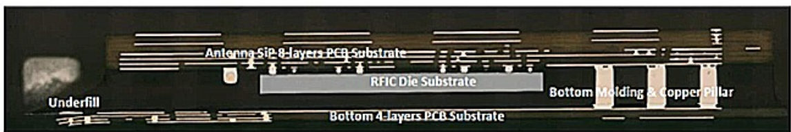
Figure 7. AiP Implementation in FEM for Asus ZenFone 4 Pro (Yole Group webcast)
Advanced packaging allows the assembly of dies (chiplets) with distinct functions at various technology nodes to achieve package-level system integration. Substrate technology is evolving continuously and becoming one of the key enablers in facilitating this trend and to experience continued market growth.


RELATED
-
Chinese top-tier chipmaker HuaHong Semiconductor's net profit plummets 86 percent in the third quarter
11-17 19:11 -
Chinese MEMS provider Fatri UTC will set up its sensor chip production plant in Shanghai
11-16 18:30 -
China's packaging and testing services provider Forehope Electronic will build a new plant with RMB2.157 billion investment
11-15 17:17
READ MOST

No Data Yet~