


By Greg Gao
JCET(长电科技), China’s largest OSAT(outsourced semiconductor assembly and test) vendor, announced on January 5 that its unique XDFOI™ Chiplet high-density multi-dimensional heterogeneous integration series process had entered the stable mass production stage as planned.
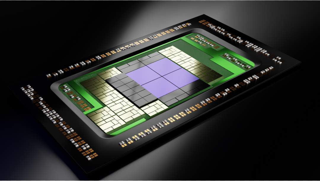
The company also shipped 4nm node multi-chip system integrated packaging products for international customers, with the largest system-in-package area of approximately 1500mm².
With the flourishing development of high-performance computing, artificial intelligence, 5G, automobiles, cloud, and other applications in recent years, the continuous innovation of chip manufacturing process is required to make up for the slowdown of Moore’s Law. The increasingly demanding high-efficiency and energy-saving chipsets through advanced packaging technologies are becoming increasingly important.
In response to the market needs, JCET officially launched XDFOI™, an ultra-high-density TSV-less fan-out packaging technology, in July 2021. It can support the integration of multiple chips, high bandwidth memory (HBM), and passive components to achieve better performance and reliability while optimizing costs; It covers 2D, 2.5D, 3D packaging and Chiplet integration technology, according to the company.
JCET’s new technology realized various high-density processes in a thinner and smaller unit area and achieved higher integration, stronger module functions, and smaller package sizes. At the same time, the technology can also carry out metal deposition on the back of the packaging materials, which can effectively improve the heat dissipation efficiency and enhance the electromagnetic shielding ability according to the design requirements, improving the yields of finished chip products, said JCET.
It will be applied in high-performance computing, artificial intelligence, 5G, automotive electronics, and other fields.
Founded in 1972 and listed on Shanghai Stock Exchange in 2003, JCET Group is based in Jiangyin, east China’s Jiangsu Province. It offers a full range of turnkey services that include semiconductor package integration design and characterization, R&D, wafer probe, wafer bumping, package assembly and final test for a global client base.
JCET has more than 23,000 employees worldwide, six production bases and two R&D centers in China, South Korea and Singapore.


RELATED
-
The IC design subsidiary of China’s listed IC distributor P&S completes testing of its first MCU product for automotive standard
11-20 16:26 -
Chinese electronic component company CETC mass produceds its Beidou satellite communication module for China’s major EV maker
11-20 15:55 -
Chinese top-tier chipmaker HuaHong Semiconductor's net profit plummets 86 percent in the third quarter
11-17 19:11
READ MOST

No Data Yet~